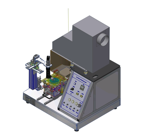
Photoresist coating
| Application range: |
*Semiconductor *MEMS *Passive Component *Touch Panel *Display Panel *LED |
|---|---|
| Specification: |
*Exposure light source: 350W、500W、1KW、2KW *Substrate Size 2”、4”、6”、8”、10”、12”-up to 24” *Uniformity: > ±3% and <±5% *Alignment Accuracy: ± 1um *Throughput:≧65 wph |
| Advantage: | Patented leveling correction mechanism/high-precision, user-friendly operation interface, module customization according to process requirements. |
| Optional double-sided alignment process: | Back Side IR (infrared light alignment) / Bacj Side Visible (back CCD/microscope alignment). |
Please fill in your contact information and the content you want to inquire, we will reply to you as soon as possible, thank you.